
Start a great journey into the core of semiconductor manufacturing, where regular sand passes through a transformation into the complex microprocessors that power up many devices today. Experience the transformation from raw materials to the complex circuits that align with today’s cutting-edge technology.
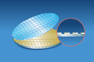
The Prominent Role of Silicon Wafers
The story unfolds with silicon, the cornerstone used in the latest electronic devices. Sourced from the common quartz-type sand, this material contains sole semiconducting qualities. With these qualities, it can serve as not just a conductor but even an insulator in some circumstances. The great adaptability suggests that it is the perfect solution for growth of the circuits that can be used in several devices to power them up. The conversion of silicon to a desired microchip wafer covers the following processes:
- Crystal development: With careful control, liquid silicon is presented into an accurately directed solidification. It then prepares a colossal crystal that is unique and shows a perfect, trusty structure. The same crystal also serves as the foundation of the thin wafers that are manufactured to support heavy-duty transistors.
- Correct Slicing: Using saws coated with diamonds, the crystal is efficiently carved into thin layers of wafers. Each layer amounts to simply a segment of a human hair’s width. Besides, these thin silicon wafers work as the cornerstone for transistor production.
- Optimal Finishing: The wafer’s exterior should be perfect to ensure there are no damages to the circuitry inside. To fulfil this objective, the wafers pass through multiple stages of polishing. Modern and reliable methods that focus on error-free machinery can make it possible to get a perfect and reliable surface.
Design for Construction of Circuit
In context to the foundation stated, the circuit design grows effectively. The preparation of outlining the design for circuit formation lets our talents align with advanced software in various ways:
- CAD (Computer-Aided Design): Engineers jointly work to effectively create the layout of the considered circuits by using CAD software. The tool results in error-free placement and easy connection of built-in billions of transistors. As a result, this approach leads to the making of a simulated blueprint.
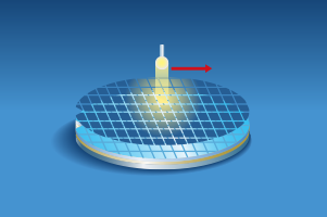
- Photolithography Procedure: This process functions like an advanced version of photocopiers. Essentially, a light-sensitive material called a photoresist is coated on the wafer’s exterior. Once this is done without any errors, a mask that includes the circuit design is placed on top. The light that passes through the openings of the mask makes the integrated photoresist harder.
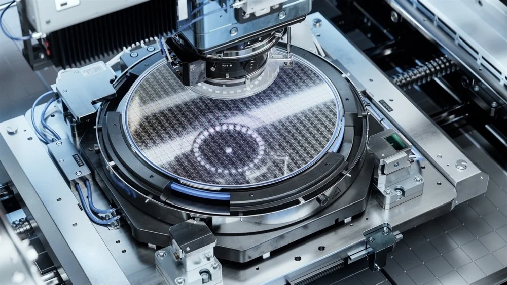
The areas freed by the mask stay rough. Afterwards, the wafer is held in a developer solution. The next step is to remove the soft photoresist material. This particular process leads to a correct overview of the circuit design cut over the photoresist material. Hence, it proves to be an error-free and reliable blueprint for the future construction of transistors.
Advancement of Layers and Transistors
Next is the construction phase, in which multiple tiny transistors are carefully built. These transistors serve as the core building components of microchips. The stages are described below.
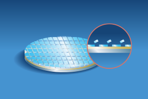
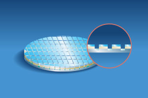
- Iterative Photolithography Process: This photolithography process gives an idea about a layered approach and repeated folds. In all iterations being taken, various materials are placed and carved over the silicon wafer. This method simplifies the development on a per-layer basis of complex circuits. Moreover, this layered method enables the development of intricate features inside the microchip.
- Inventive Approaches in Laser Technology: With the reducing size of the transistors with each passing day, today’s engineers continuously look for methods to increase accuracy. With methods such as focusing laser beams through a water layer, just the way sunlight passes through a magnifying glass, engineers can boost the overall power of the beam.
Specifically, this creative and valuable work method enables the development of similar transistors that would be multiple times thinner than the average width of any human hair. It is important to note that constructing machines that work at this level of accuracy is not easy. Due to the complex nature of such advanced technology, such water-based laser tools could actually demand a few or even several months to come together and function properly.
Key Aspects of Precision Manufacturing
The microchip manufacturing environment mainly focuses on cleanliness, wherein each component performs an important role. The same is outlined below.
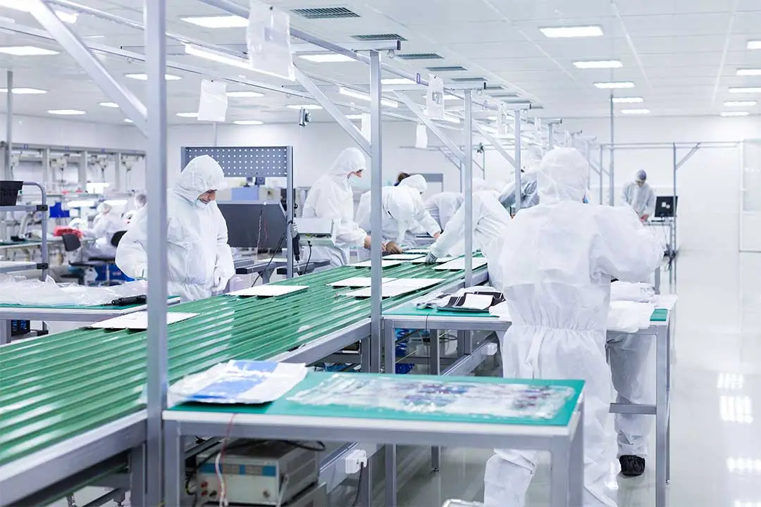
- Clean Room Devoid of Contamination: The tiniest particle of dust can damage the high-quality circuitry. But it is important to avoid this kind of damage and therefore, workers wear clothing like astronauts do. The air present in the room is repeatedly cleaned so that it becomes a lot cleaner compared to an average working room. The thorough approach to cleaning the room guarantees that the room is perfect for the development of such transistors.
- Interconnection of Copper: This process focuses on placing a thin copper layer over the wafer. The resultant layer serves as a system of microscopic wires that help in connecting nearly billions of transistors over the chip. This relevant process adopts dependable cleaning and deposition methods to guarantee reliable and proper connections in the particular circuitry.
Steps Involved in the Semiconductor Manufacturing Process
This content explains the complex world of semiconductor production. It exactly describes steps that convert raw silicon wafers into efficient microchips that takes the maximum advantage of our technology.
-
Cleaning as the Key Foundation

The first step is spotless cleanliness. Silicon wafers are the core of microchips. They need intricate cleaning to avoid any damage. It is done so that even the smallest part of dust cannot disturb the delicate circuits. Furthermore, chemical agents accurately remove all bits of particles, organic residue, as well as, natural oxides. So, ultimately, by doing this, a clean canvas is required for the next masterwork.
-
Process of Film Deposition
A wide range of methods are used to place thin film layers over the wafer’s surface. Such films will, in the end, turn out to be the important parts of the microchip. The process covers some methods like:
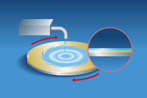
- Sputtering: It involves blasting a target material with several ions to free up atoms that cover the wafer.
- Electrodeposition: A method widely used to prepare layers of copper wire for connects in the chip.
- Chemical Vapor Deposition (CVD): It covers a combination of special gases to establish a chemical reaction, which creates a material that must be placed over the wafer.
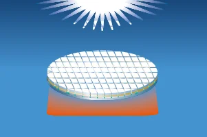
- Thermal Oxidation: It indicates warming up the wafer to create a silicon oxide film over its particular surface.
-
Maintenance of Precision after Deposition Cleaning

Once the deposition process of each film is complete, even the minor particles connected to the wafer can create issues. For the same, to guarantee a high level of accuracy, it is necessary to use brushes and nanospray having deionized water. Alternatively, using alternate physical cleaning methods can remove any residual particles.
-
Resist Coating
Resist, a light-sensitive chemical that is effectively placed over the wafer’s surface. The wafer is rolled to make a consistent layer of resist via centrifugal force. Essentially, this layer serves as a short-term mask for the next patterning procedure.
-
Design Transfer
This stage shows the benefits of converting the circuit design. It means that powerful UV rays are placed via a specially prepared mask over the resist-finished wafer. The particular includes the fine details of the blueprint of a particular circuit. It makes sure that only those regions of the resist that are facing the light will face a structural change. Hence, this step effectively transfers the circuit pattern over the specific wafer.
-
Design Etching and Development
In this stage, the wafer is being sprayed with a developer solution. The specific solution melts the parts of the resist layer which were formerly facing the light throughout the above step. The residual resist, now carved with the desired circuit design, works as a mask for the upcoming step, i.e. etching.
-
Etching

It indicates two key etching methods being used to shape the required circuit patterns over the particular wafer:
- Wet etching: It selectively removes the thin film by using chemicals such as phosphoric or hydrofluoric acid.
- Dry etching: Bombing the considered wafer surface using ionized atoms will take away unnecessary film layers.
-
Ion Implantation
To provide silicon substrate the semiconducting properties it needs, impurities such as boron ions or phosphor ions are fixed into the considered wafer. The expert presence of impurities changes the specific regions’ electrical conductivity, allowing the development of transistors.
-
Activation of Implanted Dopant Ions
In this stage, heat treatment with the assistance of either laser radiation or flash lamps leads to the presence of the dopant ions. Its activation process is important for creating the micro transistors across the particular silicon substrate.
-
Resist Stripping
The resist layer has worked as a short-term mask during the patterning processes. This stage takes off that layer. The same is done using wet stations with the help of either resist-removal chemicals or ashing (a procedure that utilizes gases to develop a chemical reaction which removes the resist). Subsequently, the wafer is cleaned again after ashing.
-
Assembly Process
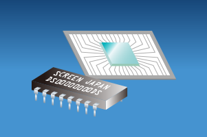
The final stage of this process is all about the transformation of the wafer into practical microchips. The sub-stages are outlined below:
- Dicing: The particular silicon wafer is exactly cut into the required chips. Each chip contains circuits and transistors.
- Wire Bonding: It effectively interconnects a unique chip to a metal frame with the support of small metal wires. Consequently, electrical-based connections are made.
- Packaging: In this final sub-stage, the chips are covered in defensive epoxy resin-type material. The key reason behind this is to offer protection and make connections to all the rest of the components within electronic devices.
This complicated process effectively transforms raw silicon wafers into modern technology. It then generates small microchips that power various devices.
Read More:
- Silicon Wafer Market to Exceed Valuation of $13.2 Bn by 2031
- How to Find a Manufacturer to Transform Ideas into Products
- Unlocking Precision: A Primer on CNC Machining
- The Semiconductor Market Will Reach Normalcy in the Coming Quarter
- The irrefutable relevance of the IoT in the contemporary world
- IoT Market is Witnessing a Notable Growth of USD 421.28 billion at a CAGR of 32.95%